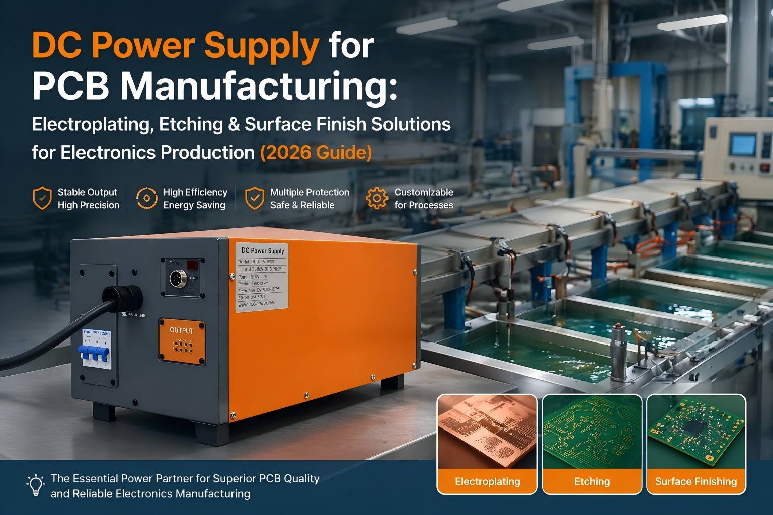
A DC power supply for PCB manufacturing is a precision rectifier system that delivers highly stable, low-ripple direct current for copper electroplating, through-hole metallization, gold surface finishing, and micro-etching processes — achieving plating uniformity within ±5% across complex PCB geometries with feature sizes down to 10 µm for advanced HDI (High Density Interconnect) substrates. In the global electronics manufacturing ecosystem — where India, Poland, and Ukraine represent rapidly growing PCB production hubs serving European and Middle Eastern markets — the rectifier’s current distribution accuracy directly determines yield rates, signal integrity, and manufacturing cost per panel.
Why Rectifier Precision Is Non-Negotiable in PCB Manufacturing
Unlike general electroplating where ±10% thickness variation may be acceptable, PCB manufacturing demands extraordinary precision. A copper layer that is 15% thicker than specified on outer layers can cause etching undercut, leading to line width reduction below design tolerances. Conversely, thin plating in through-holes creates high-resistance vias that compromise signal integrity at GHz frequencies — a defect that may pass electrical testing but fail in the field under thermal cycling.
According to IPC-6012 (Qualification and Performance Specification for Rigid Printed Boards), class 3 (high-reliability electronics) requires copper plating thickness in through-holes to meet a minimum of 20 µm with less than 10% variation. According to IEC 61683 on power system efficiency measurement, the rectifier technology choice significantly affects both plating quality and energy consumption in continuous PCB production lines.
The global PCB market is projected to reach $96 billion by 2028, with the Asia-Pacific region accounting for 85% of production. However, emerging production hubs in India (driven by government “Make in India” initiatives) and Eastern Europe (serving European supply chain diversification) are creating significant demand for high-quality PCB manufacturing equipment, including precision rectifier systems.
PCB Electroplating Processes and Power Requirements
| Process | Function | Current Density | Voltage | Key Quality Metric |
|---|---|---|---|---|
| Copper Panel Plating | Bulk copper build on outer layers | 1.5-3.0 A/dm² | 3-8V | Thickness uniformity ±5% |
| Copper Pattern Plating | Copper build on circuit features | 1.5-2.5 A/dm² | 3-6V | Distribution ratio ≤ 2.5:1 |
| Through-Hole Plating | Copper metallization of vias | 1.5-3.0 A/dm² | 3-8V | Throwing power ≥ 80% |
| Gold Plating (ENIG) | Surface finish, wire bonding | 0.5-1.5 A/dm² | 2-5V | Gold thickness 0.03-0.08 µm |
| Tin-Lead or Tin Plating | Etch resist or solderability | 1.0-2.0 A/dm² | 2-5V | Alloy composition control |
| Micro-Etching | Surface preparation | 0.5-1.5 A/dm² | 2-5V | Removal rate 0.3-0.8 µm |
Critical Rectifier Specifications for PCB Plating
Output Ripple: The #1 Quality Factor
In PCB copper electroplating, ripple content directly affects throwing power — the ratio of plating thickness in the center of a through-hole versus the surface. High ripple (>3%) causes preferential deposition at high-current-density areas (panel edges and features) while starving low-current-density areas (through-hole centers). According to industry data, reducing ripple from 8% (typical SCR) to below 1% (high frequency IGBT) improves through-hole throwing power by 15-25%.
For advanced HDI and IC substrate manufacturing with micro-vias below 100 µm diameter, ripple must be maintained below 0.5% — a specification only achievable with synchronous rectifier technology or pulse-reverse plating capabilities.
Current Density Programming
Modern PCB plating lines use programmable current density profiles that change during the plating cycle. A typical copper through-hole plating profile includes:
- Strike period (0-30 seconds): Low current density (0.5-1.0 A/dm²) to establish uniform initial nucleation on the electroless copper seed layer
- Ramp period (30-120 seconds): Gradual increase to operating current density
- Plate period (30-90 minutes): Full current density for bulk copper deposition
- Optional pulse-reverse: Alternating forward and reverse current for improved throwing power in high-aspect-ratio vias
The rectifier must execute these profile transitions smoothly without overshoot or oscillation — any transient exceeding 5% of setpoint can create visible quality defects on finished boards.
Pulse-Reverse Plating Support
For advanced PCB manufacturing, pulse-reverse plating (PRP) has become the gold standard. PRP alternates between forward current (cathodic plating) and brief reverse current (anodic dissolution), achieving superior throwing power in high-aspect-ratio through-holes and micro-vias. The rectifier must support:
- Forward pulse: 10-100 ms at operating current density
- Reverse pulse: 1-10 ms at 10-30% of forward current
- Frequency: 10-500 Hz depending on via geometry
- Duty cycle control: Independent adjustment of forward/reverse ratios
Technology Comparison: Which Rectifier for PCB Manufacturing?
| Parameter | SCR Rectifier | High Frequency IGBT | Synchronous Rectifier |
|---|---|---|---|
| Output Ripple | 5-12% | 1-3% | <0.5% |
| Current Regulation Accuracy | ±2-3% | ±0.5-1% | ±0.2-0.5% |
| Efficiency (at 6V output) | 72-78% | 85-90% | 92-96% |
| Power Factor | 0.65-0.75 | 0.95-0.99 | 0.98-0.99 |
| Pulse-Reverse Capability | No | Limited (up to 50 Hz) | Full (up to 500 Hz) |
| THD at Input | 25-35% | <5% | <3% |
| Cost Premium (vs SCR) | Baseline | 30-50% | 60-80% |
| Best For | Basic single/double-sided PCBs | Multi-layer, standard HDI | Advanced HDI, IC substrates, PRP |
QEEHUA Rectifier — Your Trusted Industrial Power Supply Partner
✓ ISO 9001:2015 Certified Manufacturing
✓ CE & RoHS Compliant Products
✓ 2,000+ Industrial Installations Worldwide
✓ Serving Clients in 80+ Countries Across 6 Continents
✓ 18-Month Standard Warranty with Lifetime Technical Support
✓ Remote Diagnostics & On-Site Service Available
Real-World Solution: Indian Multi-Layer PCB Manufacturer
An Indian multi-layer PCB manufacturer near Pune was experiencing yield losses of 12-18% on 12-layer HDI boards with 0.2mm micro-vias. Root cause analysis identified two primary issues: inadequate throwing power in through-holes (center thickness only 60% of surface thickness) and copper thickness non-uniformity across panels causing over-etching on thin areas and under-etching on thick areas.
Their existing SCR rectifiers (8% ripple, ±2.5% regulation) were the limiting factor. After upgrading to QEEHUA’s HFP-PC series 3,000A synchronous rectifiers with pulse-reverse plating capability, they achieved:
- Through-hole throwing power improved from 65% to 88% — exceeding IPC class 3 requirements
- Panel-level copper uniformity improved from ±12% to ±4% — eliminating etching-related defects
- Overall yield increased from 82% to 96% on 12-layer HDI boards, worth approximately $340,000 in annual recovered revenue
- Energy cost per panel reduced by 28% due to synchronous rectifier’s 94% efficiency at 6V output versus 75% for the old SCR units
Optimizing Your PCB Plating Line?
Get a customized technical comparison based on your PCB types, production volume, and quality requirements.
FAQ: DC Power Supply for PCB Manufacturing
What type of rectifier is best for PCB copper electroplating?
For standard multi-layer PCBs (4-8 layers), high frequency IGBT rectifiers with ripple below 3% provide excellent quality and efficiency. For advanced HDI boards with micro-vias, IC substrates, or when using pulse-reverse plating, synchronous rectifier technology is recommended for its superior ripple performance (<0.5%) and precise current regulation (±0.2%).
What is pulse-reverse plating and why does it matter for PCBs?
Pulse-reverse plating (PRP) alternates between cathodic (plating) and brief anodic (dissolution) current pulses. This improves throwing power in high-aspect-ratio through-holes by preventing diffusion-limited plating at the hole center. PRP can improve through-hole copper uniformity by 20-40% compared to DC plating.
How much ripple is acceptable for PCB plating rectifiers?
For standard PCBs (line/space ≥ 100 µm), ripple below 3% is acceptable. For fine-line PCBs (line/space 50-100 µm), ripple below 1% is recommended. For advanced HDI and IC substrates (feature size <50 µm), ripple must be below 0.5% to ensure consistent plating quality.
Can one rectifier serve multiple PCB plating baths?
While technically possible with switching, it is not recommended for different chemistry baths (copper vs gold vs tin) due to contamination risk. A common practice is to dedicate one rectifier per chemistry type but allow the same rectifier to serve multiple tanks of the same chemistry through sequential switching.
What power rating do I need for a PCB plating line?
For copper panel plating: calculate based on panel size, number of panels per rack, and current density. A typical 18″ × 24″ panel requires 150-300A at 2.0 A/dm². A 6-panel rack needs 900-1,800A. Add 25% margin: 1,125-2,250A minimum. Through-hole and pattern plating require similar calculations but with different current density values.
How does rectifier efficiency affect PCB manufacturing costs?
At the low voltages used in PCB plating (3-8V), efficiency differences between rectifier technologies are amplified. An SCR rectifier at 75% efficiency consumes 33% more electricity than a synchronous rectifier at 96% for the same plating output. For a medium-scale PCB factory running 24/7, this can translate to $15,000-40,000 in annual energy savings.
What standards apply to PCB plating rectifiers?
Key standards include IEC 62477-1 (power electronics safety), IEC 61000-6-2/4 (EMC immunity and emission), IPC-6012 (PCB qualification requirements), and IPC-A-600 (acceptability of printed boards). Rectifiers used in electronics manufacturing must meet CE compliance and should be RoHS-compatible for European market access.
For PCB manufacturers in India, Poland, Ukraine, and other emerging electronics production hubs, selecting the right precision DC power supply technology is a strategic investment that directly impacts yield, quality, and cost-per-panel. QEEHUA’s rectifier solutions for PCB manufacturing are designed with the specific requirements of modern electronics production in mind.
Ready to Upgrade Your PCB Plating Power Supply?
Our PCB application specialists will analyze your current setup and recommend the optimal rectifier configuration.